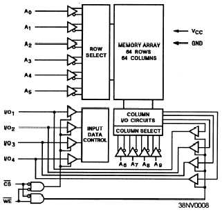
block diagram of a 1K by 4 is shown in figure 6-31.
This RAM chip uses 10 address lines to address 1024
words. The address is provided over 10 input lines (A0
through A9). The 10-bit address is internally translated
within the chip. Bits A6 through A9 feed the column
select circuits while bits A0 through A5 feed the row
select circuits. The address lines are used to enable the
addressed memory cell flip-flop circuits by row and
column number. The 10 address lines form 210, or
1024, possible conditions. Each addressed word has 4
bits.
There are 4,096 memory cell flip-flop circuits in a
64 row by 64 column memory array. Within the
64 by 64 memory array, only 4 flip-flops enabled by
both row and column signals can be set or cleared by
the data bits during a write operation or can have their
outputs sensed during a read operation.
Data is stored in, or read from, the memory cells via
the four I/O lines, I/O1 through I/O4. To provide stable
signals within the memory cell array, the four I/O lines
are buffered, as shown on the block diagram. The
address lines are usually tied to the computer or memory
system address bus, while the I/O data lines are tied to
the data bus. The I/O lines are bidirectional. For write
operations, they carry the data to be written into the
memory cells.
For read operations, they carry the
output of the memory cells.
The remaining pin connections shown on the block
diagram are used for control and power. The chip select
line is an input used to enable a particular part, or
example, a 16K by 8 memory can be from 32 of the
1K by 4 static RAM chips. Only two chips are selected
during any single read or write sequence. The chip
select
signal, when tree, indicates that the
particular chip’s circuitry has been selected for a read
or write operation. The chip select signal originates
from a higher level decoder circuit, which controls
several RAM chips. Common address and data lines
connect all the chips under the decoder but only the chip
receiving the chip select will handle the data.
The write enable
input line is used to
determine whether a read or write operation is taking
place. The write enable signal is generated from the
computer system. When the chip select is active, a write
pulse on the write enable line is used to store data within
the memory cell array. The internal circuitry of the chip
will accept data from the I/O lines and set or clear the
selected row and column flip-flops to match the bits on
the I/O lines. The data buffers are switched to input
mode during a write cycle. During a read cycle, the
write enable is false indicating that the read cycle is
being processed and the data buffers are switched to the
output mode. During a read operation, the internal cell
data is output to the computer data bus. The contents
of the flip-flops themselves are not changed by the read
operation.
The VCC and ground lines are used to supply power
to the memory IC. Power consumption varies slightly
with the mode of operation of the static RAM. Atypical
1K by 4 static RAM uses 5 volts of dc power, and
typical power consumption is 500 mW.
group of parts, out of a large memory array. For
Dynamic RAM (DRAM)
Figure 6-31.—Block diagram of a 1K × 4 SRAM.
Dynamic random access memories (DRAMs) are
semiconductor integrated circuits (ICs) that operate like
a bank of capacitors.
DRAMs consist of MOS
transistors. Figure 6-32 is an example illustration of a
dynamic RAM cell and its associated circuitry. The
cells are capacitor-type circuits; a charged cell equals a
logic 1, while a discharged cell equals a logic 0. Each
cell consists of a MOS transistor and a tiny capacitor.
When a row-line is activated, all the MOS transistors
on that row are turned on, connecting their capacitors
to their column lines. Byway of the column lines, the
capacitors are charged when writing and the charges are
detected when reading. Electric charges are put into the
cells through the column lines and read out through the
same lines, using appropriate switching circuitry in the
column selector section. Words from the data input in
figure 6-32 are written into the capacitors through the
column lines and the data is readout through the same
6-24


