cycles. One uses an external refresh and the other an
internal refresh.
Dynamic RAM Organization and Operation
Our example dynamic RAM chips both have 64K
of memory. We label them dynamic RAMs A and B.
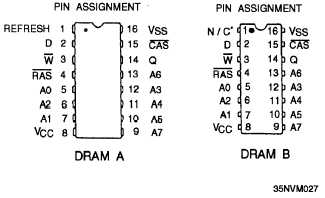
Dynamic RAM A contains a built-in refresh circuitry,
which is driven by a simple external clock, while
dynamic RAM B must be refreshed by external logic.
A pin-assignment diagram for these DRAMs A and B
is shown in figure 6-33.
These dynamic RAM parts contain 65,536 1-bit
words and require a 16-bit address word (216= 65,536).
The address word is formed by a multiplex technique;
whereas two 8-bit words are input in two steps from the
eight address lines labeled A0 through A7. This 8-bit
word must be formed by external logic that interfaces
the computer memory bus to the memory system.
The D line is the data input line. The Q line is the
data output line. These lines may be tied together or
separated; it varies with the system. The D and Q lines
are tied together in
applications that call for a
bidirectional data bus. However, separated D and Q
lines speed up the system. In larger memory systems,
all the dynamic RAM parts in the memory array share
the address bus.
The data bus is separated into
individual data bits. Each bit is associated with one
RAM Chip.
For timing and control, the system uses the refresh
address strobe
and the column address strobe
lines. To signify when a write operation is being
performed, the system uses a low level on the
The
VCC pin is used for 5 V power input. The VSS is held
at ground.
Figure 6-33.—DRAMs with pin assignments: A. DRAMA with
built-in refresh circuitry; B. DRAM B which requires
external refresh logic.
6-26
On DRAM A, pin 1 is used for refresh. The pin 1
refresh technique uses an internal 8-bit counter to
generate the required 128 refresh addresses. Use of this
pin requires a low-state clock pulse on the refresh line,
while the RAS signal is sent to a high state. The refresh
clock increments the refresh address with each clock
pulse. With external logic, this technique is fairly
inexpensive. The main disadvantage of this IC is the
additional internal refresh logic.
The alternate refresh technique can be used on both
DRAMs A and B. This alternate technique uses the
RAS and CAS lines to control the refresh mode. The
RAS line is sent low, while the
line is sent high,
and the refresh address is presented from external logic
to the DRAM memory array. All 128 refresh addresses
must be presented within two milliseconds, as is the
case for the self-refresh mode.
TOPIC 3—READ-ONLY MEMORY
(ROM)
In modem computers, portions of the available
main memory addresses and special local memories are
made up of read-only memory (ROM). ROMs are used
for various memory applications, such as fixed program
storage, look-up tables, and code conversions. The
programs on the ROM are actually more hardware than
software; therefore, they are often referred to as
firmware. ROM has all the operational characteristics
of read/write memories except that data cannot be
written into the ROM addresses by the normal computer
accessing methods (write request). You can only read
and/or execute the contents of each ROM memory
address. The contents of the ROM addresses can be
used over and over again without alteration, and the data
does not have to be written back into ROM. The
primary use of a ROM allows the computer to perform
its I/O operations, which is one of the primary functions
of the CPU. In this chapter, we discuss how ROM
works and the different types of ROMs; how and when
they are programmed.
The term non-destructive
readout (NDRO) memory is often used to describe ROM
used in militarized computers. Newer computers use
ROM and the different variations of ROM in the NDRO
to store the bootstrap and other special-purpose
programs.
READ-ONLY MEMORY (ROM)
ARCHITECTURE
ROM is consistent in all computers. Remember it
is tailored to meet each computer’s needs. ROM comes


