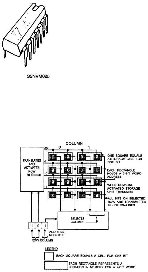
Figure 6-24.—RAM chip.
of variable numbers of these RAM chips. Each chip
contains large numbers of memory cells and the logic
to support them. Each memory cell is an electronic
circuit with at least two stable states. With the advent
of large and very large scale integration (LSI/VLSI),
literally thousands or hundreds of thousands of memory
cell circuits can be placed on a single chip. Each of the
two-state memory cell circuits is capable of storing a
single binary digit orbit (0 or 1).
Figure 6-25 shows the general idea of how one-bit
storage units (or cells) of any type are typically arranged
so that stored information can be read out at random.
The same arrangement works for writing data into a
RAM. Notice the row and column arrangement; this is
the same concept used by magnetic read/write
memories.
As a simple explanation, look at the
memory shown in figure 6-25. It stores only 16 bits, as
eight words of two bits each; notice the
row-and-column arrangement. These chips are
mounted on logic boards or circuit card assemblies
pcb’s) in some sort of memory array, also called gate
arrays, based on the memory capabilities required or
desired by the equipment designer.
The capabilities of individual chips determine the
array organization for the memory capabilities desired.
On RAM chips, memory cells are organized based on
two factors, the number of memory words or
addresses and the number of bits per word. Most
memory logic chips are rated by these values. For
instance, a 4K by 16 chip would provide 4,096 16-bit
memory addresses. This 4K by 16 chip will not support
a 32-bit word for 4,096 addresses. The best it can do is
the lower or upper half of the word. To support a 32-bit
Figure 6-25.—One-bit storage units.
6-21


